WEEK
EIGHT
ELECTRONIC PRODUCTION
Task for this week
Group Assignment
Characterize the design rules for OUR in-house PCB production processIndividual Assignment
Make and test the development board that we designed to interact and communicate with an embedded microcontrollerGroup Assignment
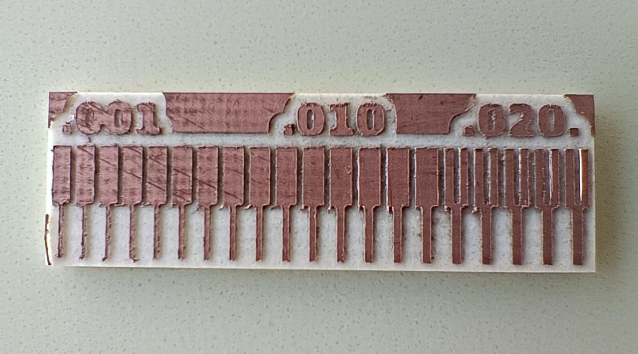
For the group asssignment we have to test the machine precison.we have Roland SRM20. It is used in many milling process. For this we download a providedpng file and generate its tool path by Modsce and then we have to Milling and cuttin this board on our machine.
Click here to know more about group Assignment.
on the basis of this design we have to select our machine parameter and set them at the time of designing.
Individual Assignment-
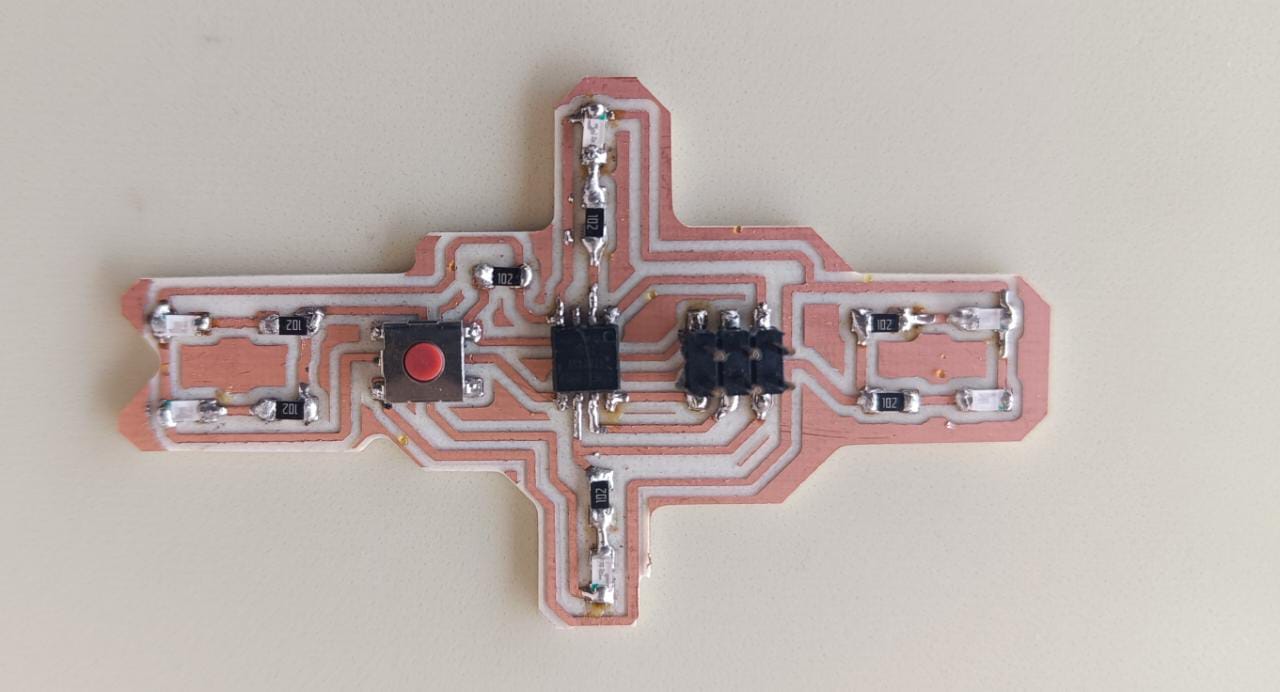
This week is for the electronic production and we have to make a PCB board which we designed.I designed a board with xiao esp32ce in previous
electronic design assignment but due to un availability of xiao board I am Not able to make it.So this week I designed a new pcb with attiny 45.
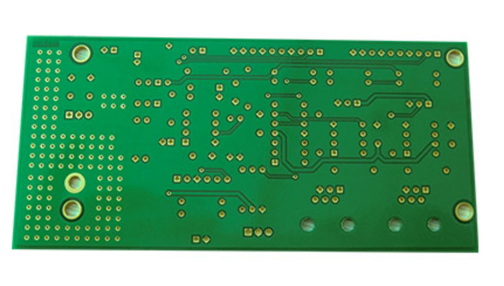
Before making PCb we have to know about the pcb maufacturing processes. PCB is the backbone of electronic industries. every electronic we use are having
a PCB in it. PCB replace the wire joint with milling pathway on the copper coated board. all the electronic component are attached on the pcb by soldering
process.This component are attached very closely thats why PCB also save the space.
PCB material
The Pcb material consist two layer. one layer is a conductive layer and another one is non conductive layer. 1.Metal- Metal layer like copper, iron and aluminium are used for pcb material. among all of them copper is most used Pcb metal because it have good conductivity to theelectricity. the selection of this metals are based on the component which is mounted on it.
2.PTFE or TEFLON- it is also used for PCB due to its propertities.it is very strong. Ptfe is flexible and lightweight and does not expand on high temperature
in other words we can say that it is fire resistant.
3.FR-4 - It is made up of flame rsesistant epoxy resin binder and oven fiberglass cloth. the FR is stand for flame retardant. The green color PCB actually made by
This material.
Types of Component-
there is two types of component for Pcb manufacturing. One is SMD (surface mount component) and other is through component.smd component required pad and through hole component required hole for assembly.
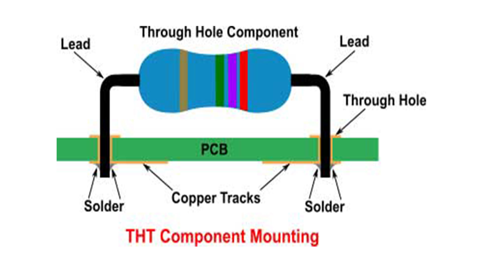
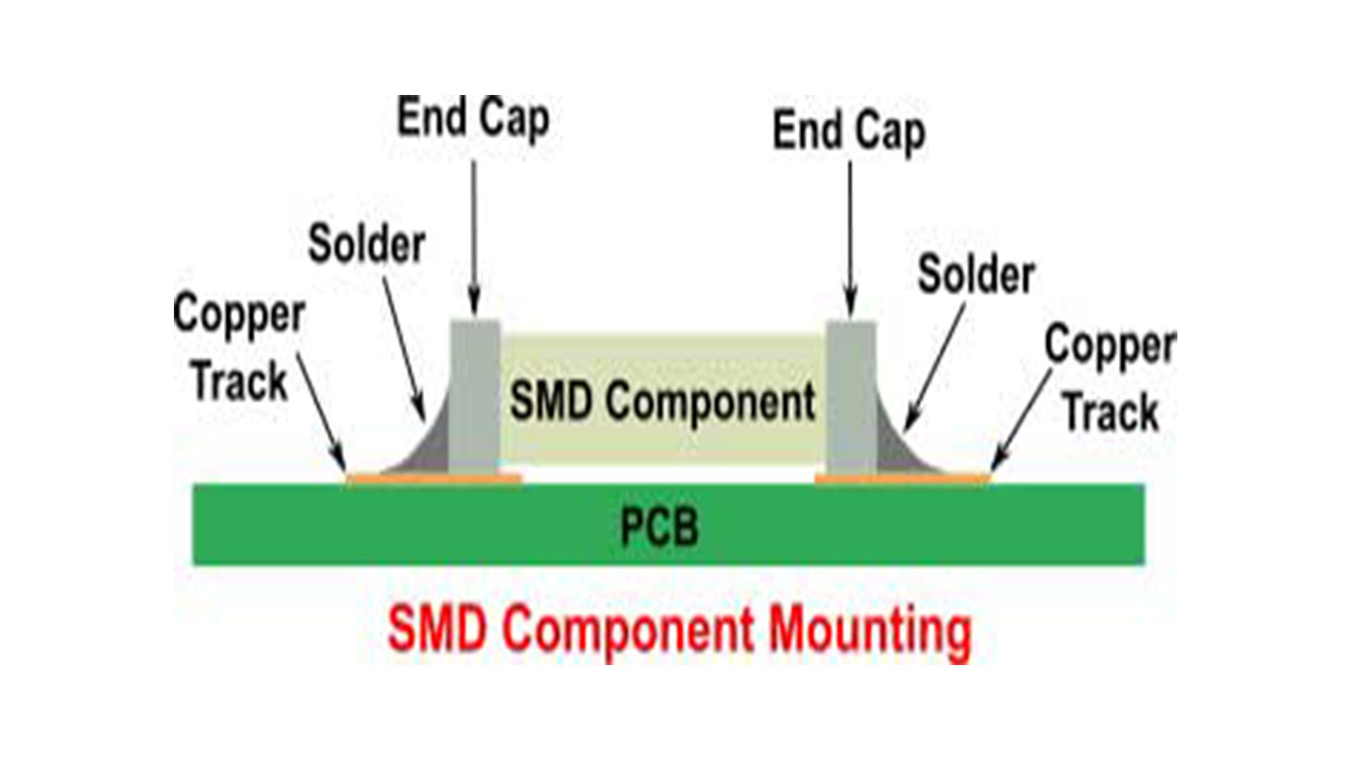
In through hole pcb we have mounted the component only one side but in Smd PCB we can mount the component on both side.
the assembly of the through hole component is done manually while the smd componenet assembly done by machining process.
It is used where board density is low and Smd component used where board density is high.
Types of PCB fabrication methods
1.PCB milling proces-In this process there is board which have upper layer with a conductive metal. We engrave this conductive layer by Milling tool.
In this process a three axis movable machine are used in which we connect the milling tool and it replace the material and generated trases.
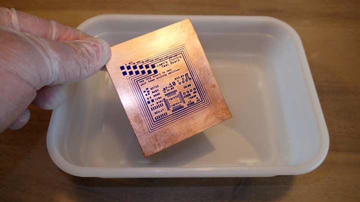
2.Etched circuit Board-
In This process we have to print our design on shiny sid eof paper then paste this paper on the copper board .
Now give some heat to the board.Afte some put this board in water until the paper is removed. Then put this board in etching solution
After some remove it and clean the surface by alcohol and then our pcb is ready .
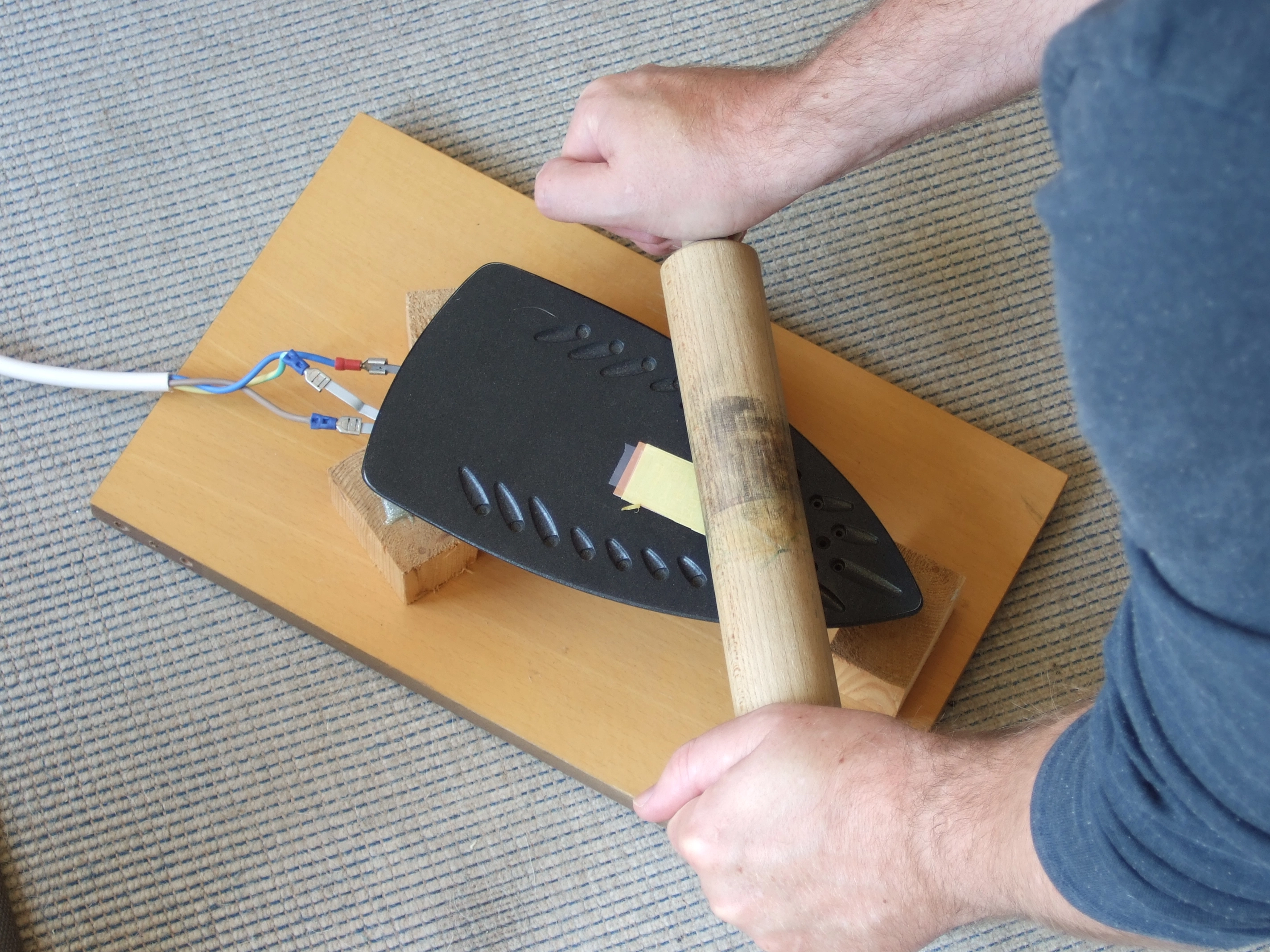
3.Toner transfered method-
In this Proccess we have to use laser printer and print the desined pcb on the OHP paper and then paste the paper
on to the board and apply heat by iron on the pcb board . After one minute we have to cool down this board and then dipped it into Etching solution
Then clean it by alcohol.
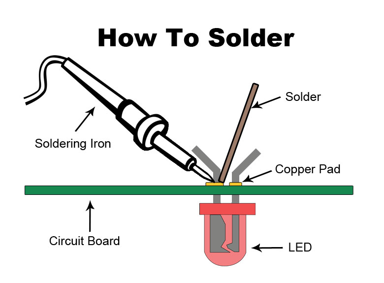
Soldering process
Soldering is the process of joining the component together to make electrical and mechanical bond. We use a low melting point alloy which is used in solderingprocess. Generally the soldering wire is alloy of lead and tin. Flux help in joining the solder stick without flux may be the soldering not proper on component.
We used a soldering iron which is heated and when the soldering wire come in contact with solder iron, The wire get melted and then we apply this melted wire on
Component.
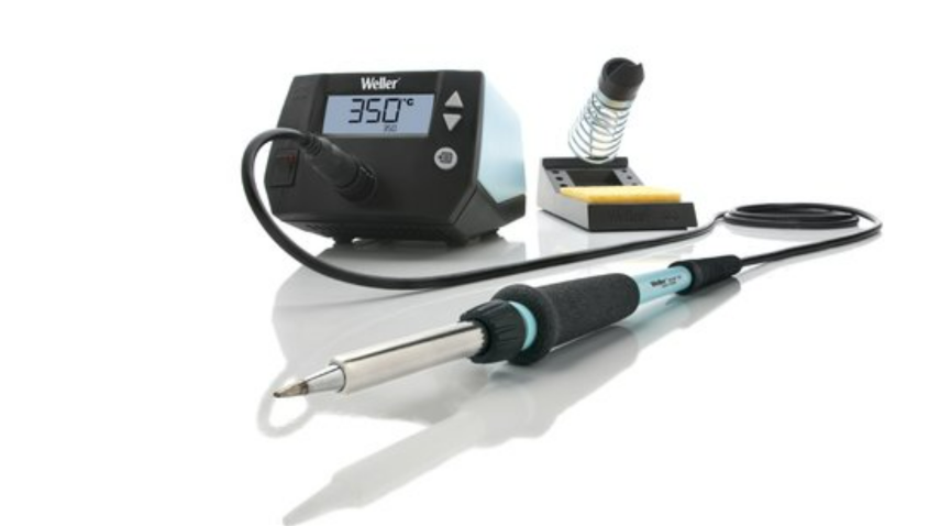
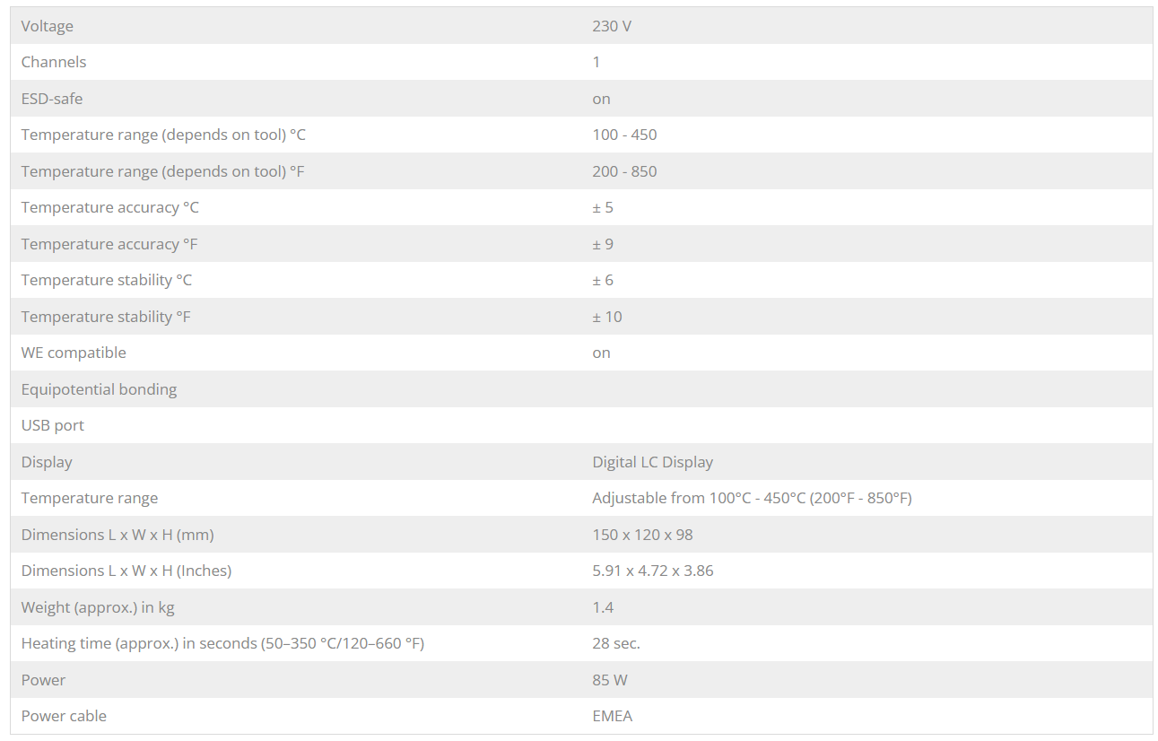
We have a weller company soldering Iron. its temperature we can according to Our Requirement.Its temperature goes down when not is use.
Machines-
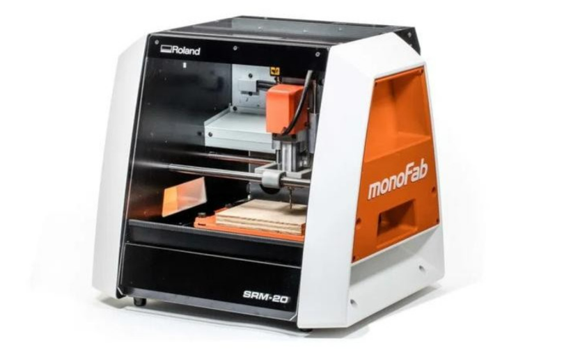
we have Roland SRM 20 Machine Manufacture a PCB. It has the working area of 203.2mm in x axis, 152.4 mm in y axis and 60.5mm in z axis.It perfome pcb milling operation and also made a a designed on the chemical wood by which can make mould of chemical wood. it can take the load about 5kg of workpiece
while working. Other details are given below -
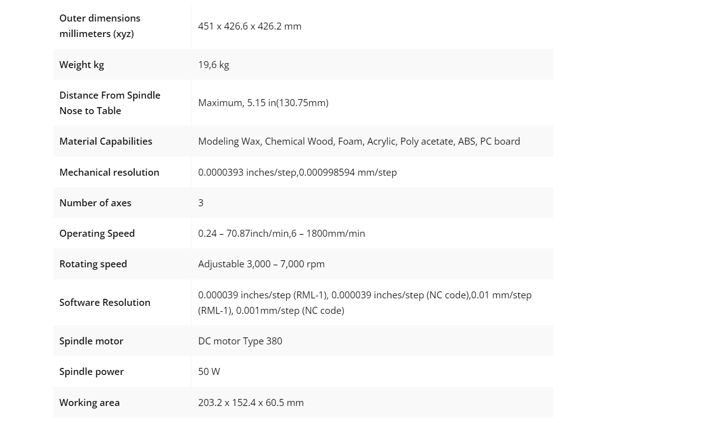
Tools-
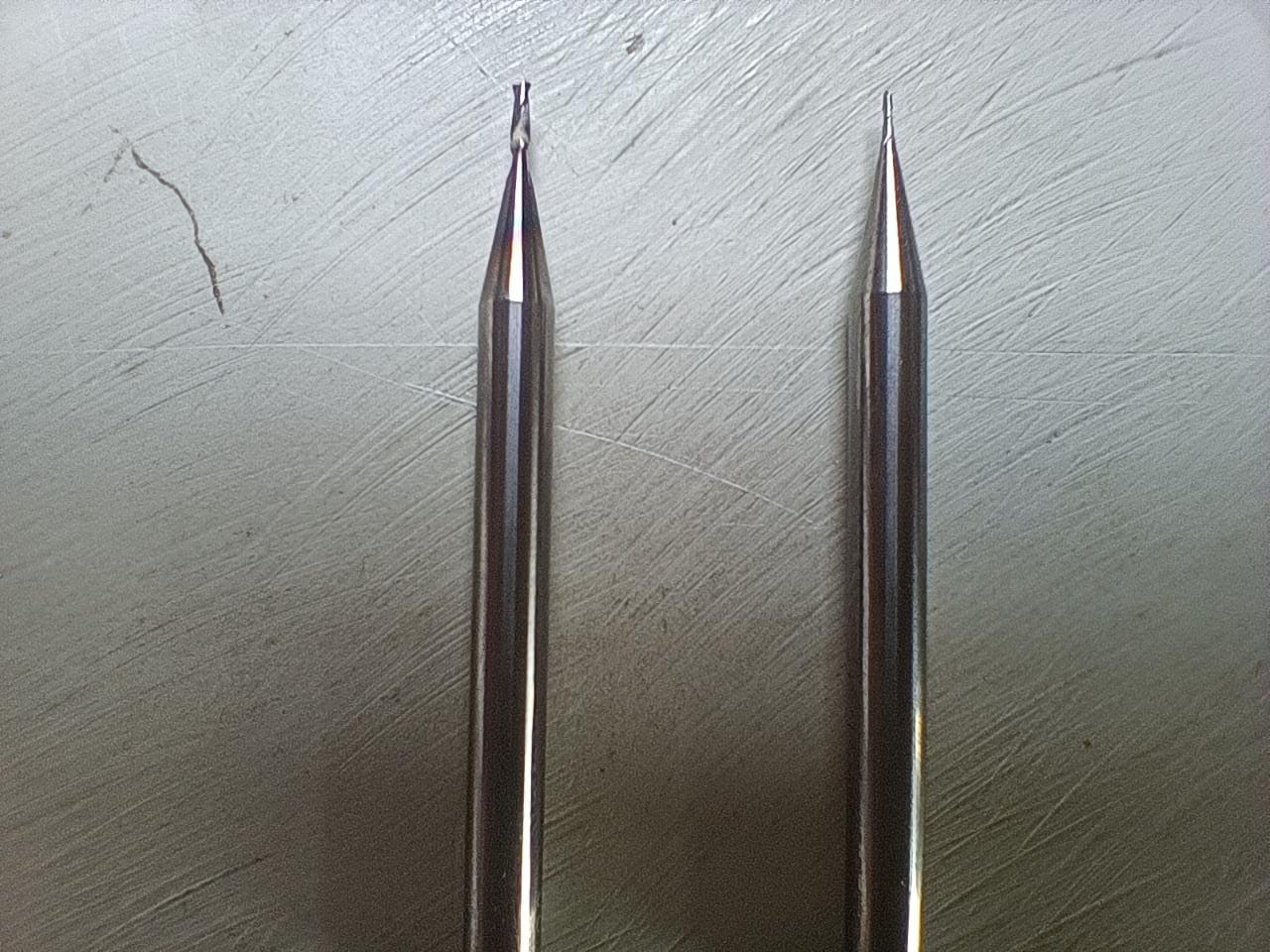
there are basically two type of tool is used in this machine. One is milling and other is cutting.
Milling tool-
we used 1/64"(0.015625") diameter tool for milling operation. Its small diameter make the fine pathway inside the PCB.Its also provide excellent details on PCB.
Cutting tool-
we used 1/32'(0.03125") diameter tool for the cutting operation. its wider diameter provide it support at the time of cutting. V-bits-
This is also a milling tool. Its have 15 Degree angle between two sharp edges. it is used when high accuracy and detailed PCB required. Its made up of alloy steel
which make it hard and rust free.
PCB production
In pcb productin we multi stage of operation. We have to complete this operation one by one. We have some steps to produce a PCB-1.Design
2.Toolpath Generate
3.machining process
4.Component Soldering
5.Programming
DESIGN
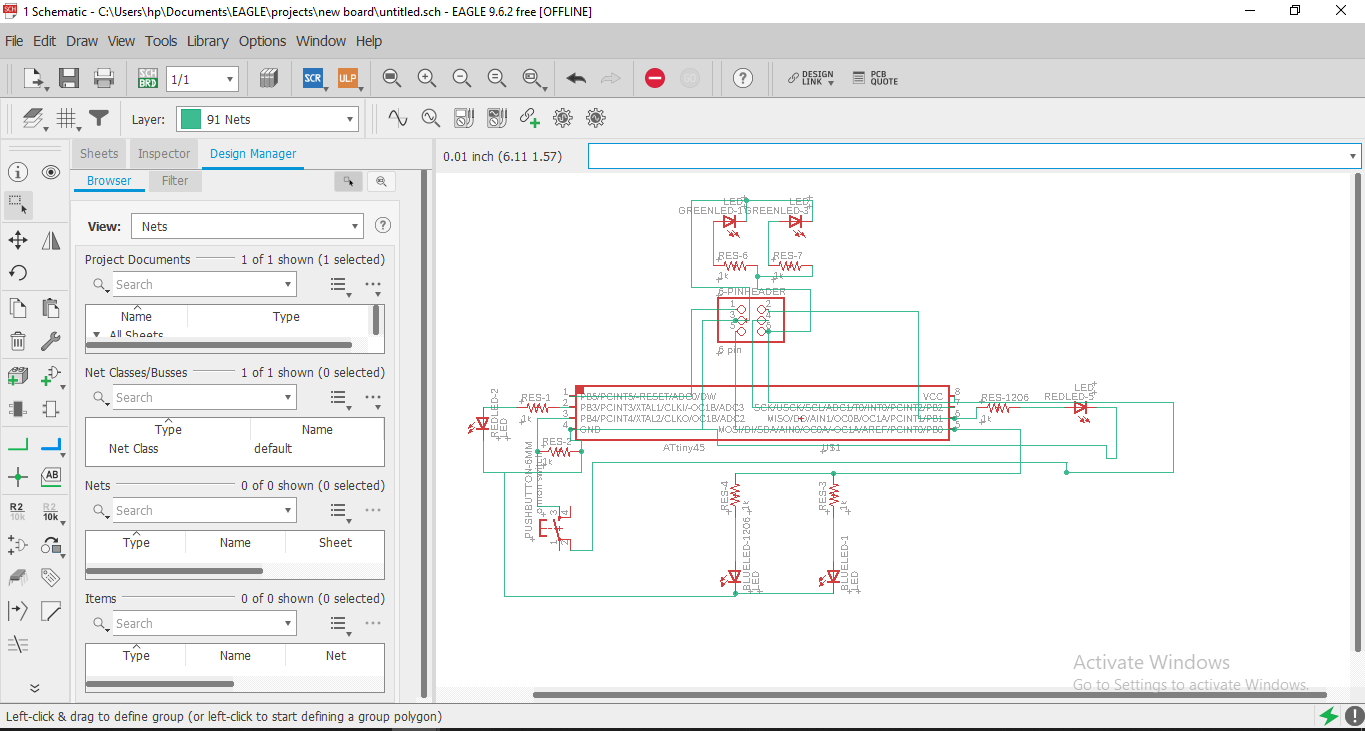
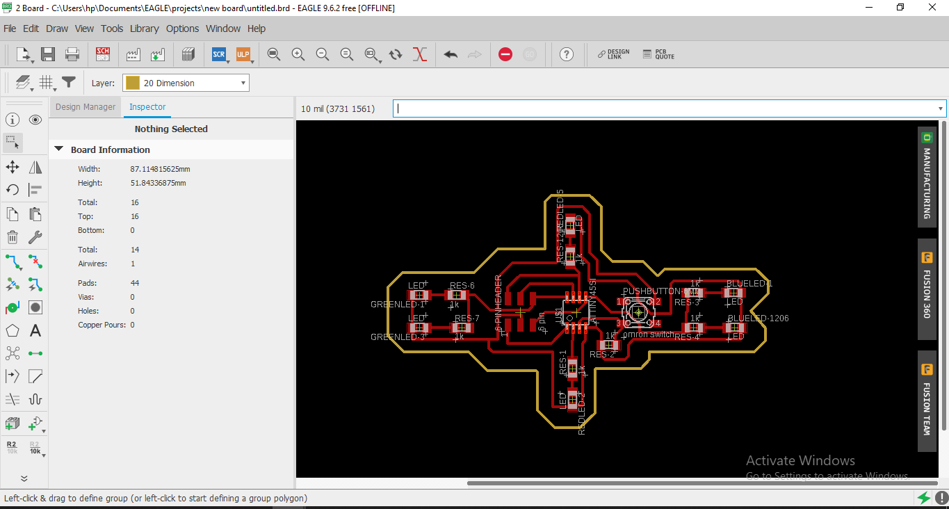
Now I mentioned above that I designed a new PCB board for this week. For design I choose Eagle.I created a new project on the eagle. Now this time I designedPCB with Attiny45. So its easy available on fab library. Now I go to add part option and select one Attiny45, 1206 package LED, 1206 package resistor , a 6 pin header and a push button.
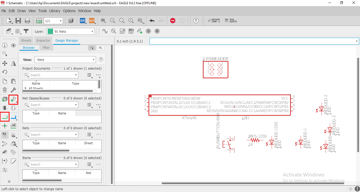
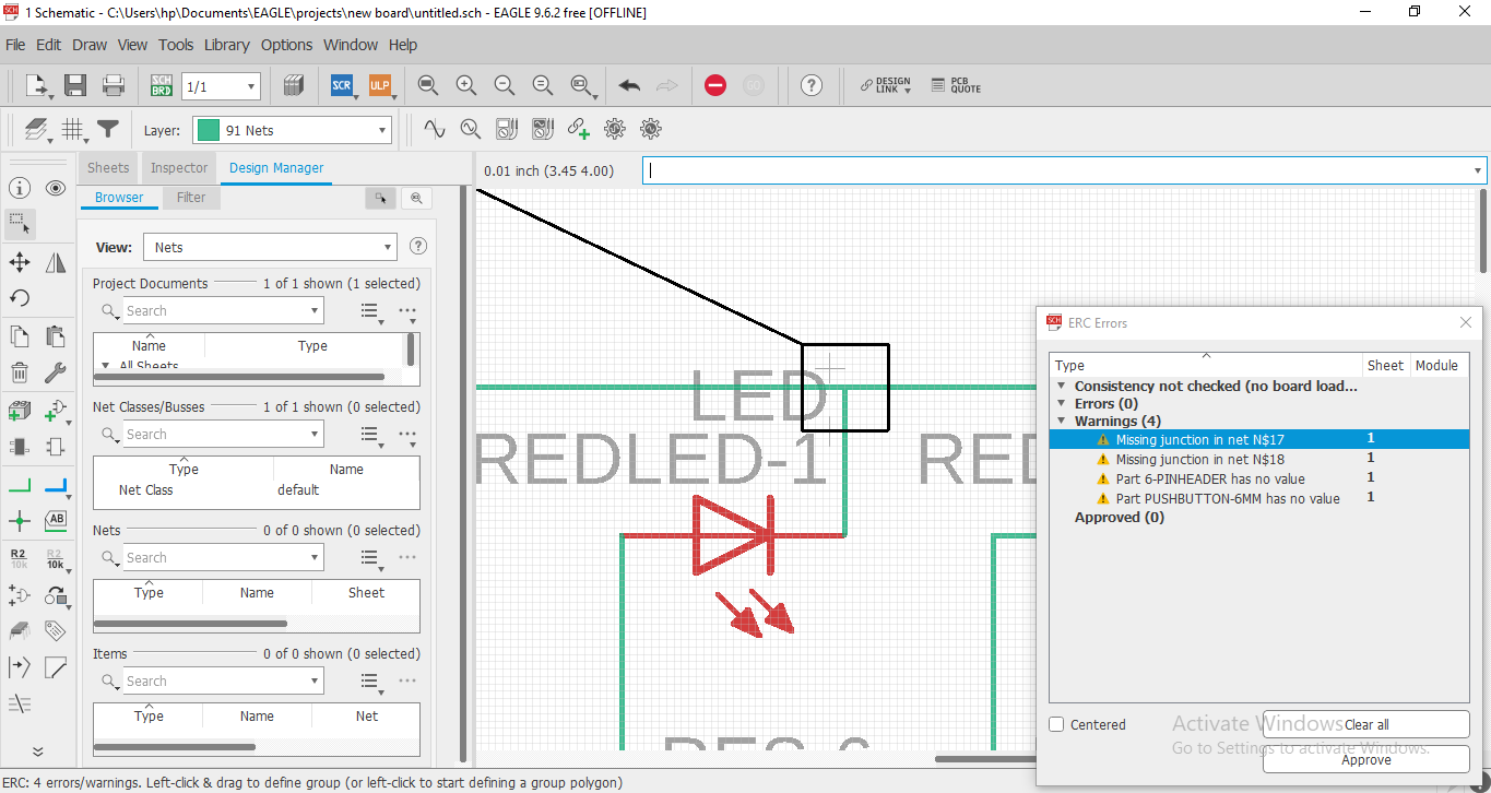
Then I arrange the component and give connection between them. After connection I checked the electronic rule check and found some unconnected component
so I connect them again.
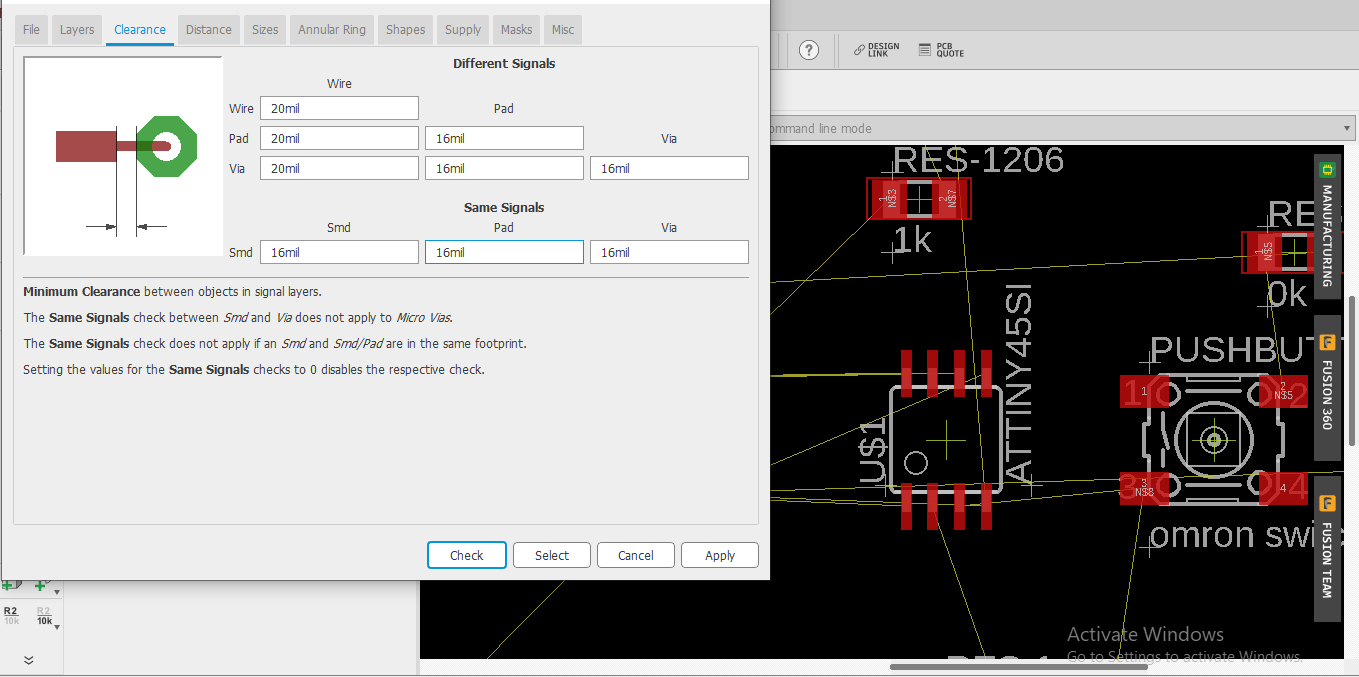
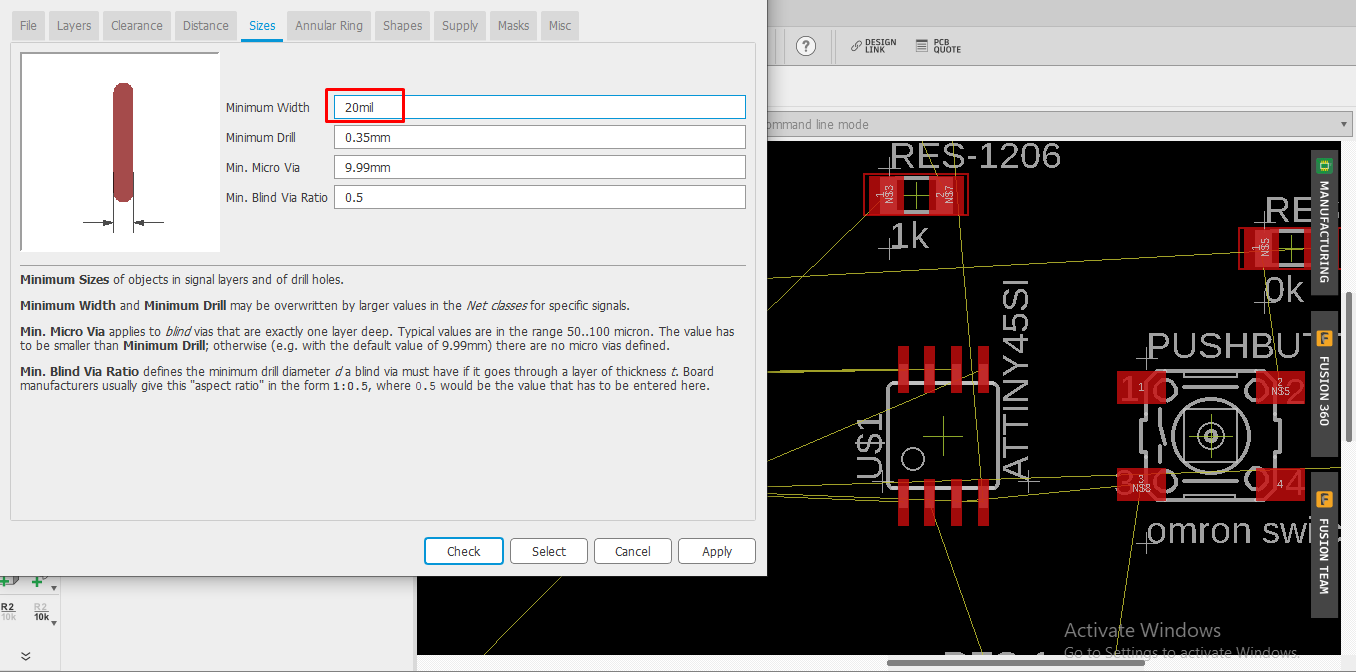
Now I changed board From schematic to Board design. Before the arrangment I setup the design rule check (DRC) and set the milling traces width and gap
according to the tool diameter. The diameter of the tool is 1/64 (=0.015625inch)
Here I have to arrange this all component in proper manner .After arranging them I trace path for component. for makinf path I used route airwire and then. I select the dimension layer
and then select line command and make its dimension or boundry layer .
Then I go to layer and hide all the layer and make visible only top and pad layer. After then I go to file and select export option. Follow this steps
Go to File >> Export >> Image
Then Select name of your file and browse the location where you want save your file. Then select monochrome and set the resolution about 1000 and then save your file.
follow the same process for the Dimension layer also. Go to layer and hide the all layer except dimension and export it by following above steps .
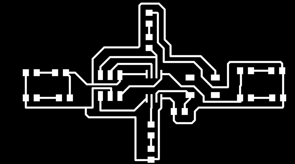
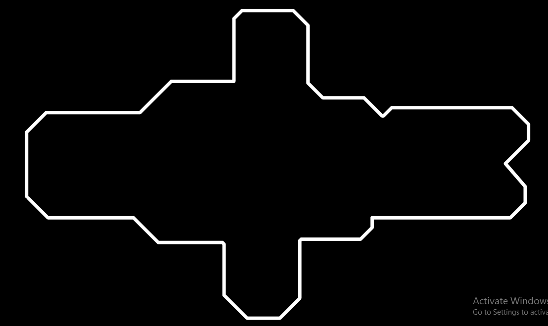
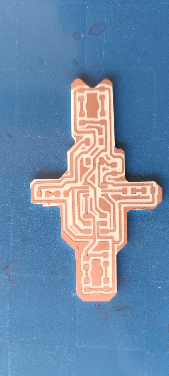
By exporting we created its PNG file which is used In milling and cutting Operation.
Toolpath Generating
There is a many software by which we can generate the toolpath for the pcb milling machine. Now we are using MODS CE platform to generate toolpath.This platform is manage by MIT-USA. By this platform we can cotrol our machine also. It create toolpath for many machines like shopbot, vinyle cutter etc.
Search the mods ce on Internet and open it . A blank window is open Then right click on the window and select program.
After this open a new program.
Here we find out our machine and enter. Now a window open which contain colorful boxes.Each box is connected with another box. All the box contain some values.
Here we have to upload our Png file. we can also upoad svg file of pcb.
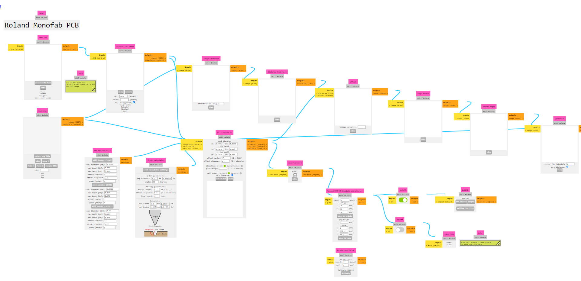
This is tool selection box. We select the tool according to our operation. we choose 1/64 for the milling operation and 1/32 for the cutting operation.
Now here we show the parameter like depth , feed speed, Tool diameter etc.
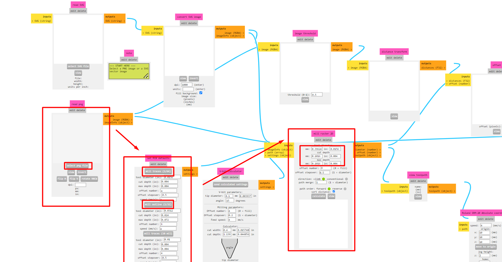
Now we can set the machine origin from this platform but most of time we set the machine origin by its cam software. for this we have to set 0 for all three axis
We can direct operate the from this but when we want download the toolpath file then we on the save file option and off the WebUSB option.
At the last we move on calculation box. here all the paprameter regarding toolpath shown here. when we click the calculate option our toolpath generating file is downloaded.
Now we open the our Png file for milling operation then select 1/64 milling tool .
then make origin of all the axis zero and on the file save option and then calculate.
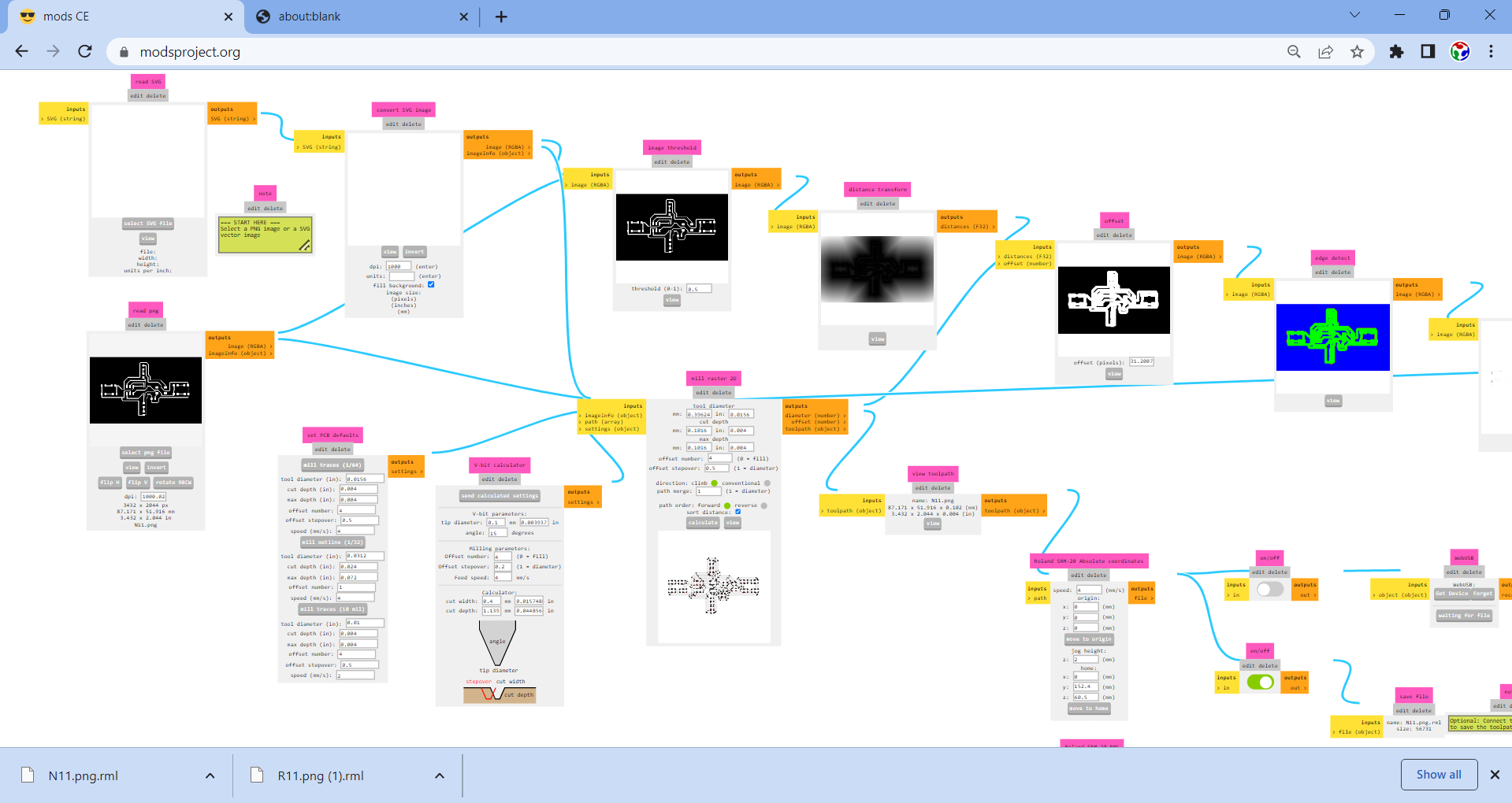
A rml file downloaded which is used in milling opearion. Now open our png file of border then select 1/32 cutting tool and follow the same process and download the rml file for cutting operation.
then again calculate the paramete and rml file downloaded for the cutting operation.
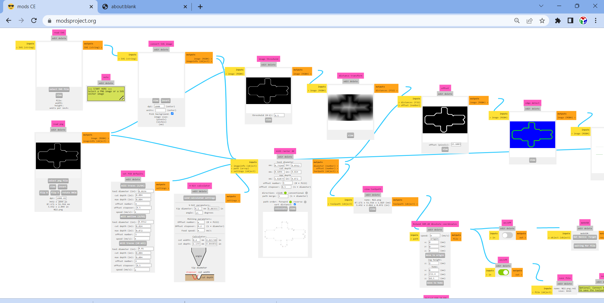
Download the rml file of the design
Download FileNOTE
I am using a FR4 board for PCB board making due to unavailabilty of FR1 board in our lab.Machinig process
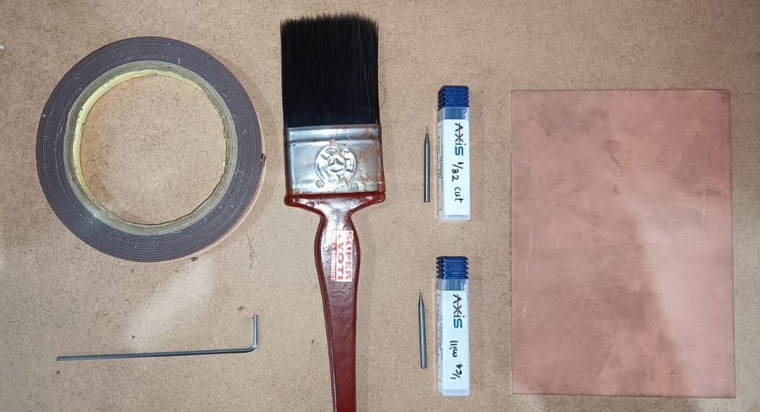
Now in machining process we milling and cutting our PCB board. before machining lets ready the initial arrangment.Things we need in machining process-
1.Copper clad Board
2.Milling and cuuting Tool
3.Alen key
4.Double sided adhesive tape
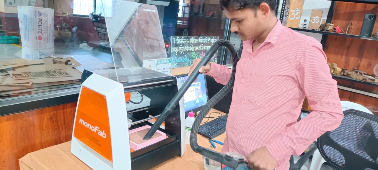
5.vaccum cleaner
6.Brush
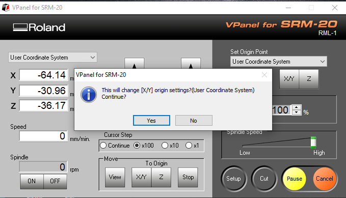
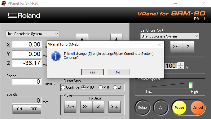
firstly powen on the machine and open the V panel software of the machine. when machine is power off the v panel cant be open . Now In software there are x, y and z axis controller are there. At the down side we set our machine tool on origin. and its cursor speed can be controlled by the
parameter. At the right side we can set a new origin point for the tool head and the down side we have some controlling option. Box1 show the axis values
Box 2 at the down side we can see the feed speed and spindle speed of the machine.
Box3-from here we can move all the three axis
Box4- From here we can decrese our cursor speed
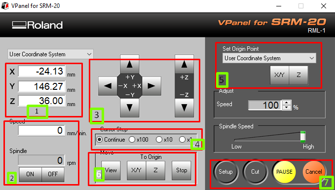
Box5-here we set the the current values of X, Y and Z axis as origin.
Box6-this is used for the movement of axis toward the origin.
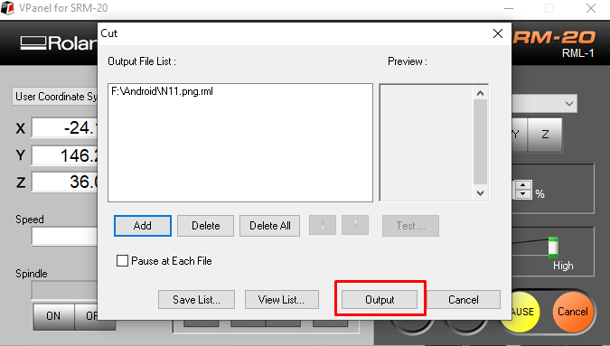
Box7-this is used for machine control at the time of operating. also it have cut option by which we select the rml file for milling and cutting.
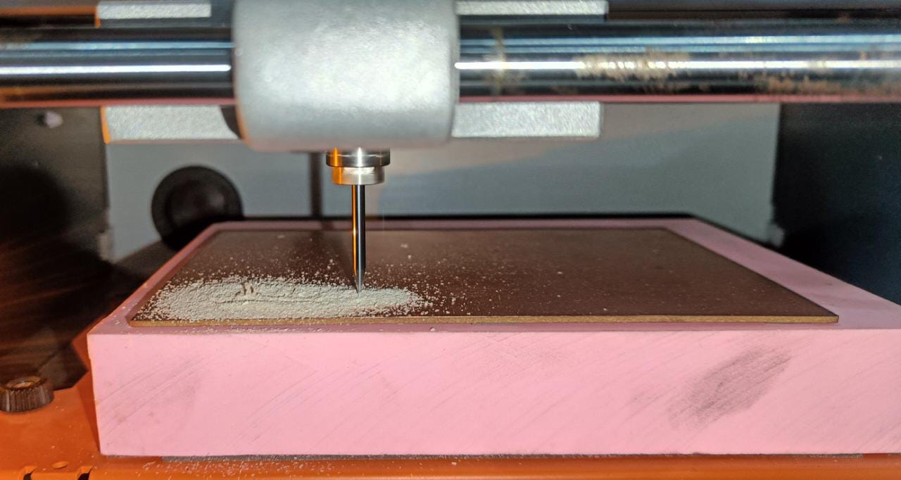
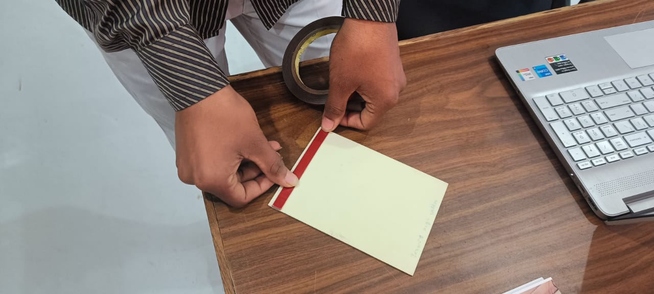
Now firstly apply the double tape on the copper board and stick them on to the machine bed. Then select 1/32 milling tool and tight it on the tool head.
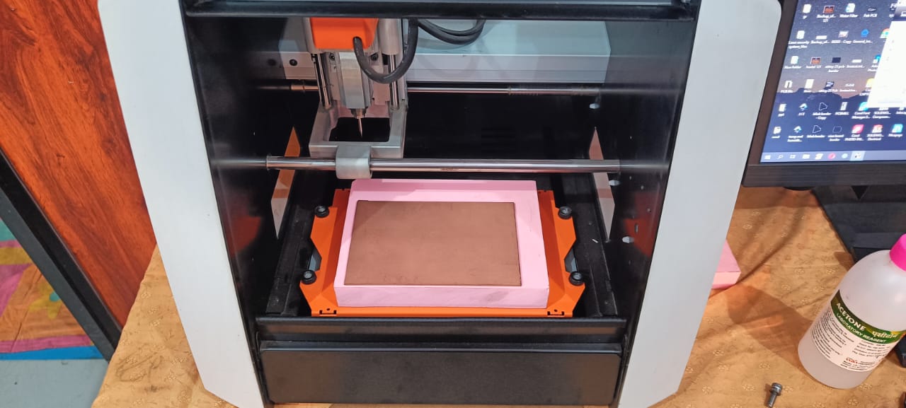
now select a origin point on the basis of x and y axis dont set z as origin. after selecting x and y axis as origin now slowly down the z axis and stop when the gap between board and tool
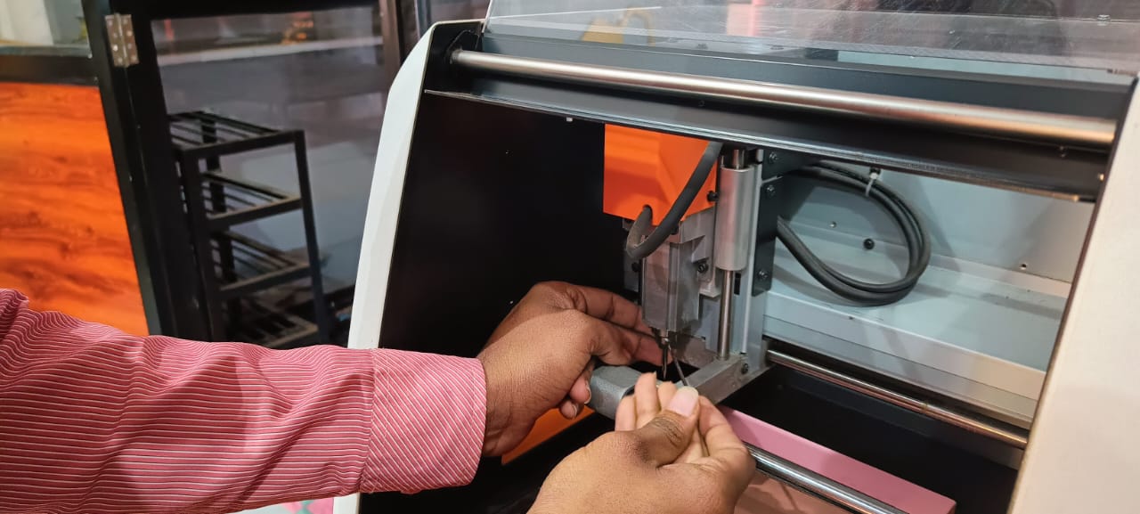
is just about 3-5 mm. Now loose the tool, it freely fall on the board then tight it agian, this is known as gravity test by which tool is perfectly come in contact with
copper board. Now select z axis as origin.
After that Go to the cut option and delete the previous file and go to add option and select the toolpath generating rml file for milling operation.
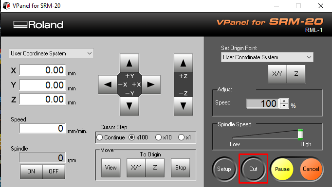
after selecting the file go to the output option and our milling process start.
when the process is completed ,use vaccume cleaner to clean the dust on board.
After milling process dont change the origin of the machine. It is very important point. we can not change the origin value of x and y axis. Now replace the tool by 1/32
cutting tool and then select move xand y to origin option. then x and y of the tool head come on origin point then select z axis slowly down the tool head. Now do gravity test for
this tool also. After test set the z axis as origin and again go to cut option, delete the previous file and select file of border cutting and go for output option.
then our cutting process of Our PCB board started. When the process is completed, clean the dust by vaccumm cleaner and safely remove the PCB board from machine .
Now apply brush on the board by which small particle also removed.
Component details
1.Attiny 45-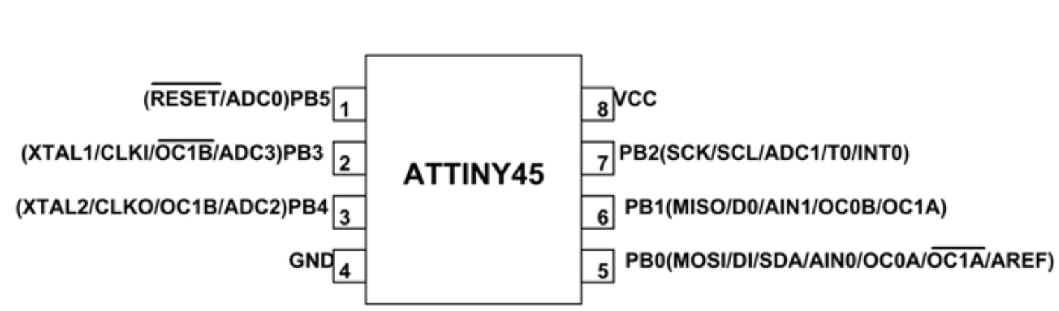 Attiny 45 is smaller microcontroller IC. It have total 8 pins.
It have 2 power pin (one is vcc which is at pin no.8 and GND which is at pin no.a)
Attiny 45 is smaller microcontroller IC. It have total 8 pins.
It have 2 power pin (one is vcc which is at pin no.8 and GND which is at pin no.a)It have 2 clock pins, 6 input/output pin, 3 SPI communication pin, 2 i2c communication pins, 6 PWM pins, 4 ADC pins.
It has 4kb of flash memory, 256b of SRAM and 256b of SROM. it operate on 5v voltage.
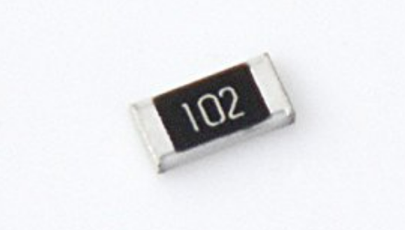
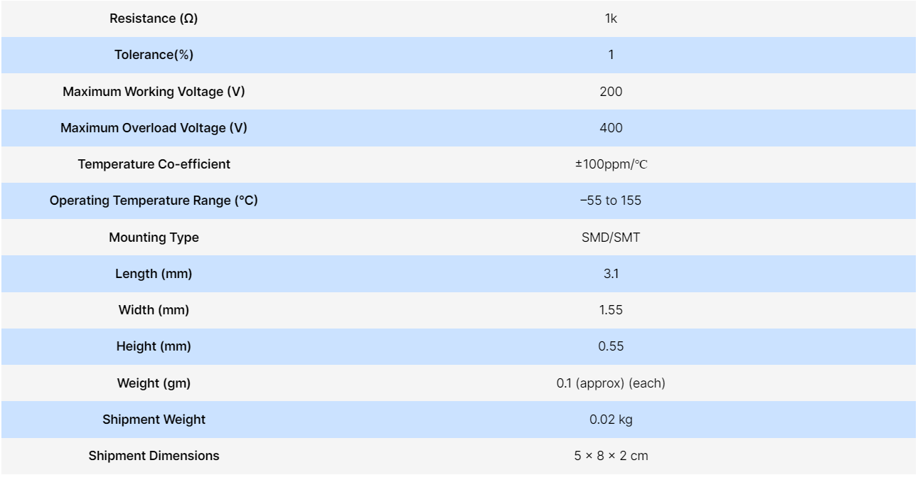
2.1206-1k SMD Resistor
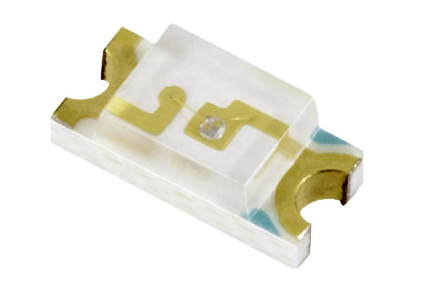
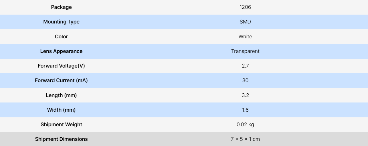
3.1206-SMD LEDs
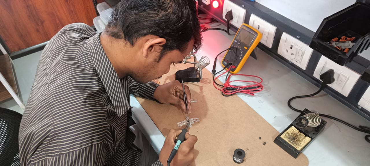
Component Soldering
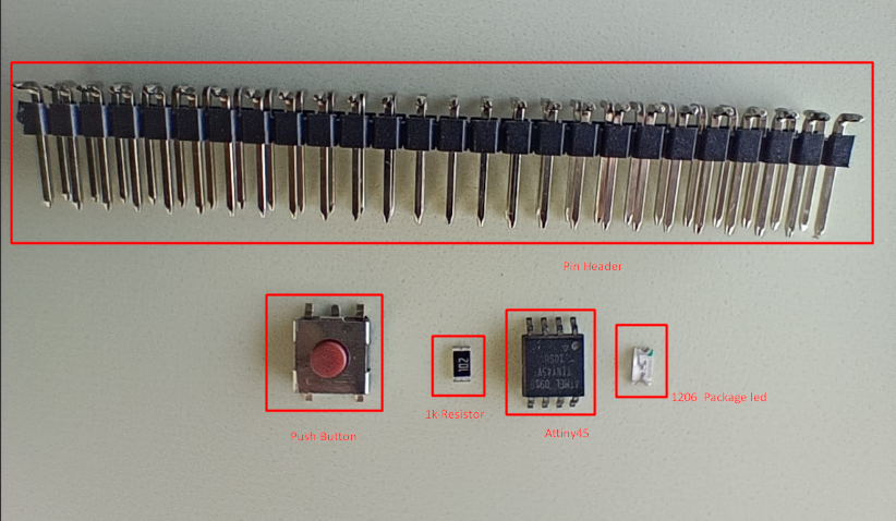
we used soldering wire which is made up of solder and it is alloy of lead and tin. Soldering wire has low melting point that why we used in our component soldering. This wire also have a flux core inside it. flux help in increse the wetting ability of solder wire by which it can spread rather than making a round ball. Now we have raedy our component list1. Attiny45- 01
2.1206 package 1K resistor -07
3.push button -01
4.pin header of 6 pin -01
5. 1206 package LEDs(2-orange ,2-green, 2-Blue)
Now I just Set my soldering iron temperature between 310 to 340 degree celcius and start soldering them. Firsltly I stick some solder on the pad
and then I soldered the component on the board one by one. solder small component first then solder bigger component.
After soldering all this component we are moving toward programming.
Programming
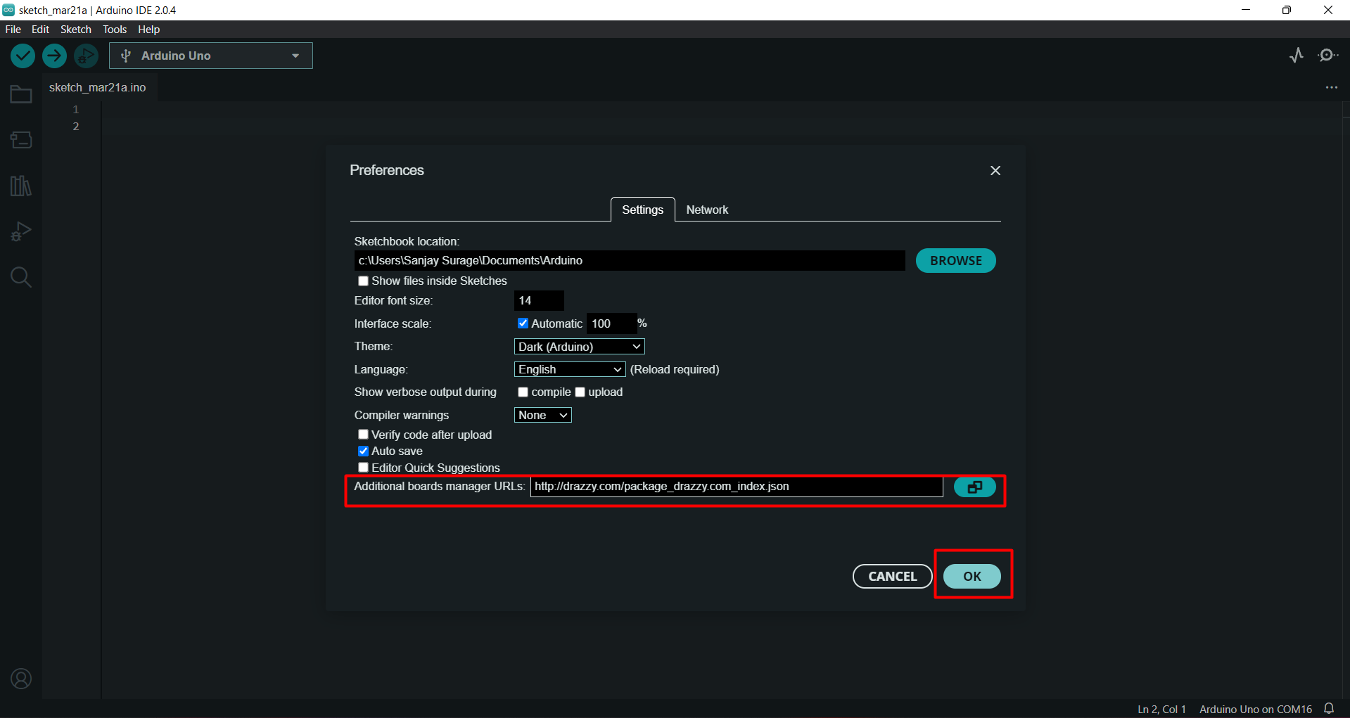
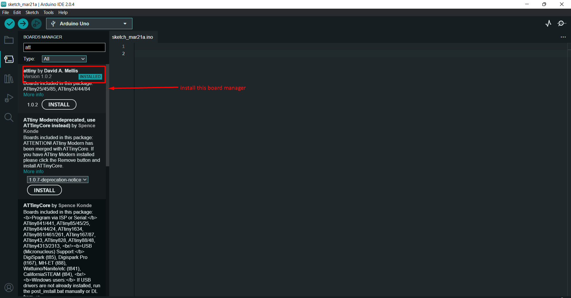
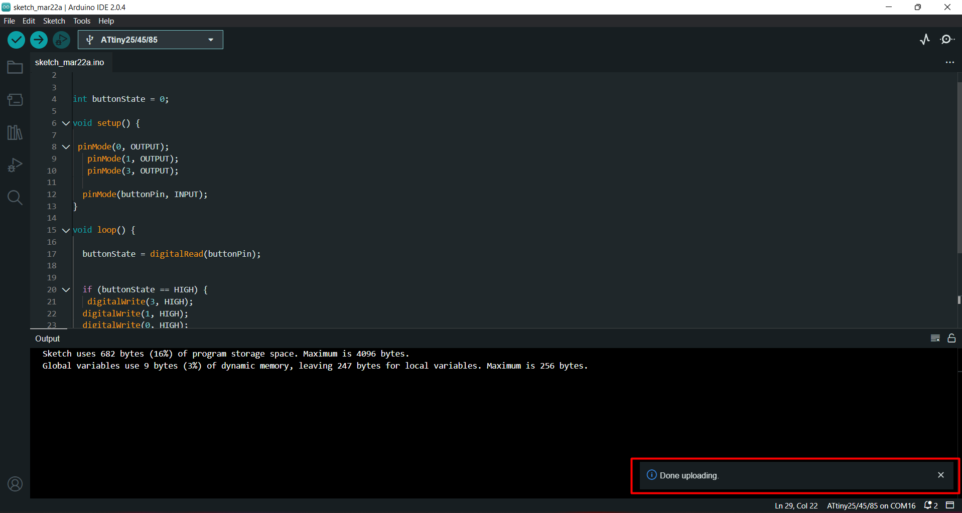
Now we have to upload programme by using Arduino. Open the arduinoIde. we have to add attiny board in the board manager. so for add board follow thesteps- Go to the file >> preference >> paste the url which I mentioned below and ok.
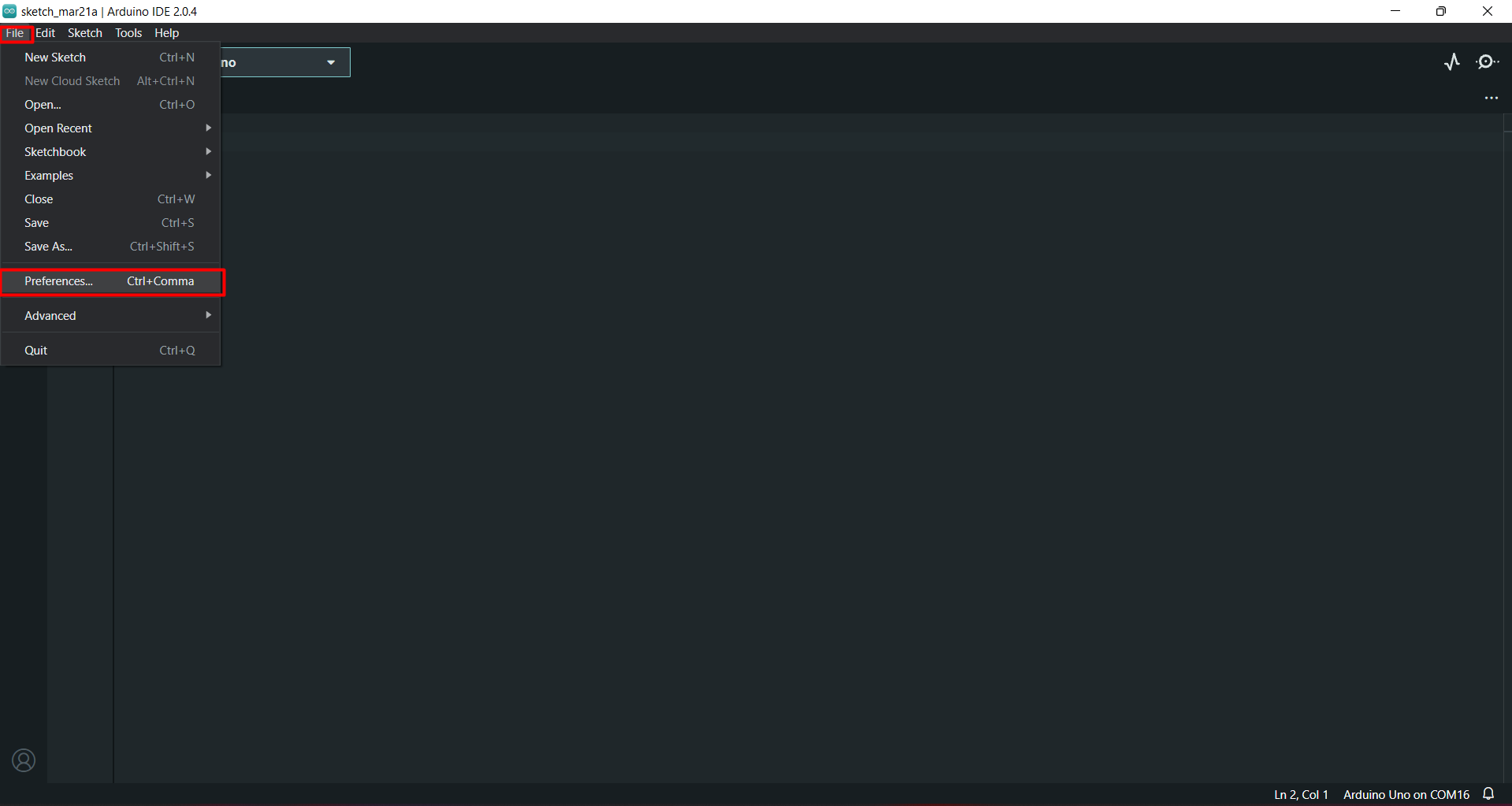
Copy This link and past in prefence in arduino ide-"http://drazzy.com/package_drazzy.com_index.json"
Now go to board manager and search attiny in serach box and select attint by david. and istall it.
After installtion go to the tool select board as "attiny25/45/85" then select processor and then select clock speed as 1mHz for Attiny 45.
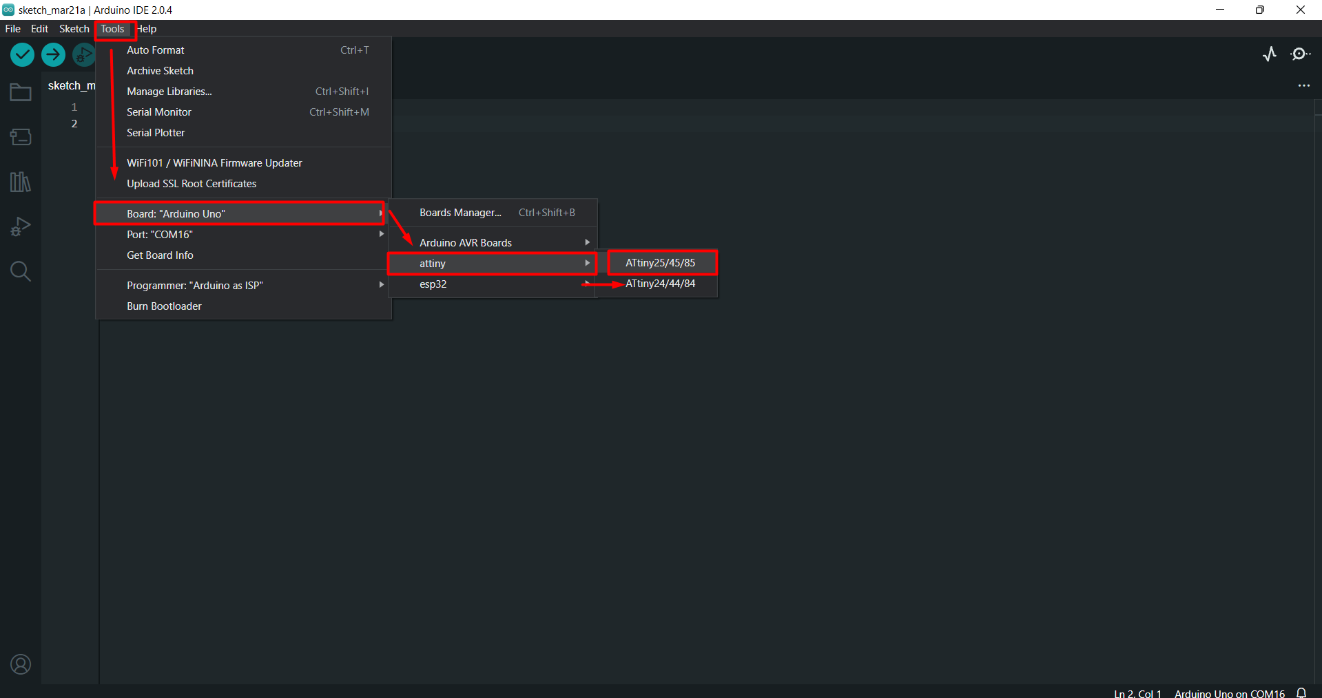
Now select arduino ISP for programmer. Then write code and compile it.I have use a blink code and do some modification on it.
Now connect our pcb board with arduino uno pin-
Miso - D12
Mosi - D11
SCK - D13
Reset -D10
5V - VCC
GND - GND
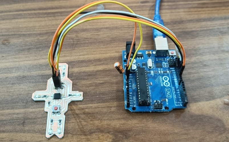
We also connect a capacitor of 10uf between the ground and reset.The negative of the capacitor connect to the ground. It prevent the arduino from reboot. after connecting all this pin go to the sketch and select "upload using programmer".
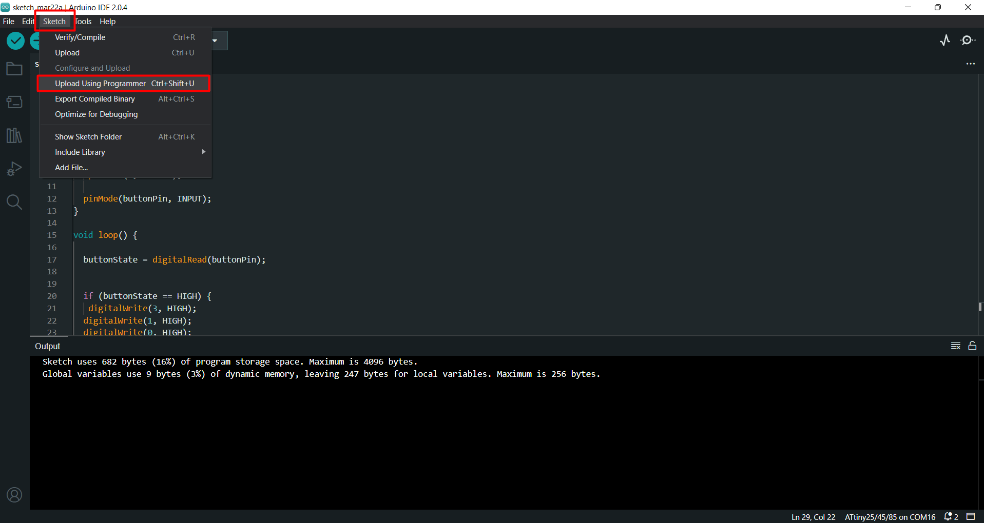
After that the programme successfully uploaded to the PCB board
Result with LED Blink
Result with pushbutton
Note
I am using a FR4 board for PCB board making due to unavailabilty of FR1 board in our lab.Learning outcomes
-I learned about the Different types of pcb Manufacturing Techniques.-I learned about the Different type of PCB material and Component
-I designed a new PCB with Attiny 45 on Eagle.
-I learned about the tool path generation and Milling and cutting operataion on SRM20
-I learned the soldering process and solder the smd component on pcb board
-I leraned about of programming for attiny45 by arduino uno.
Download the all original file
Download FileClick here to know more about group Assignment.